


 226 / 300

TSC-0912 - 09.10.12
Furse, Wilford Road, Nottingham, NG2 1EB • Tel: +44 (0)115 964 3700 • Email:
enquiry@furse.com• Web:
www.furse.comESP PCB/E Series
Suitable for wave soldering
Very low let-through voltage (enhanced protection to BS EN 62305)
between all lines - Full Mode protection
Full mode design capable of handling partial lightning currents as well
as allowing continual operation of protected equipment
Repeated protection in lightning intense environments
Very low (1
Ω
) in-line resistance for resistance critical applications
High (1.25 A) maximum running current
Higher bandwidth enables higher frequency data communications
2 pin clean end and 3 pin line end to ensure correct insertion
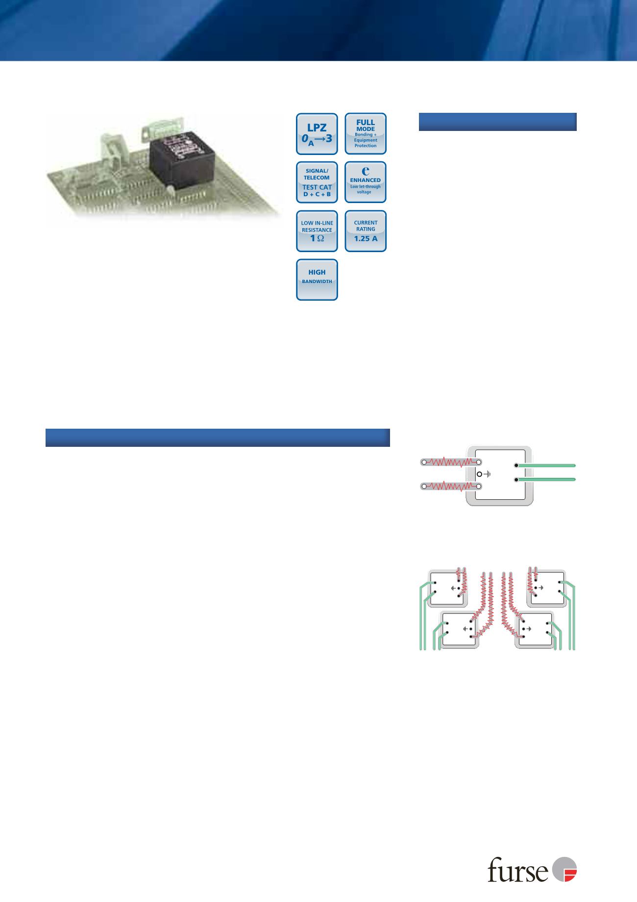
Features and benefits
Combined Category D, C, B tested protector (to BS EN 61643) for
“through hole” mounting directly onto the PCB of data communication,
signal or telephone equipment which require a lower in-line resistance,
an increased current or a higher bandwidth than the PCB/**D Series.
Available for working voltages of up to 110 Volts for AC & DC power
applications up to 125 Amps. For use at boundaries up to LPZ
0
A
to
protect against flashover (typically the service entrance location)
through to LPZ 3 to protect sensitive electronic equipment.
Connect in series, soldering pins
direct onto PCB. Tracks to line and
earth pins should be as wide as
practical (see Furse
Application
Note AN003
).
Dirty (line) tracks should be
routed parallel and as close
together as possible. This should
also be implemented on clean
tracks, however clean tracks
should never be routed close and
parallel to line tracks or dirty
barrier earth connections as
transients can be re-introduced
after the protector due to
electromagnetic coupling.
The use of an earth layer or
plane is highly recommended as
this reduces the electromagnetic
field produced by a transient
discharging to earth considerably,
and hence the chance of the
transient being picked up on
clean tracks.
Installation
Maximum line to clean separation. Large input
tracks and pads (using top and bottom copper
layers). Earth pin is bonded to an earth
layer/plane.
All dirty (line) incoming tracks are separated from
the clean output tracks, individual line and clean
tracks are routed close together. Earth pins are
bonded to an earth layer/plane.
Clean
1 3
4
2
Line
Line
Clean
Clean
3
4
3
4
1
2
1
2
ESP PCB/**
3
4
1
2
ESP PCB/**
1 3
4
2